
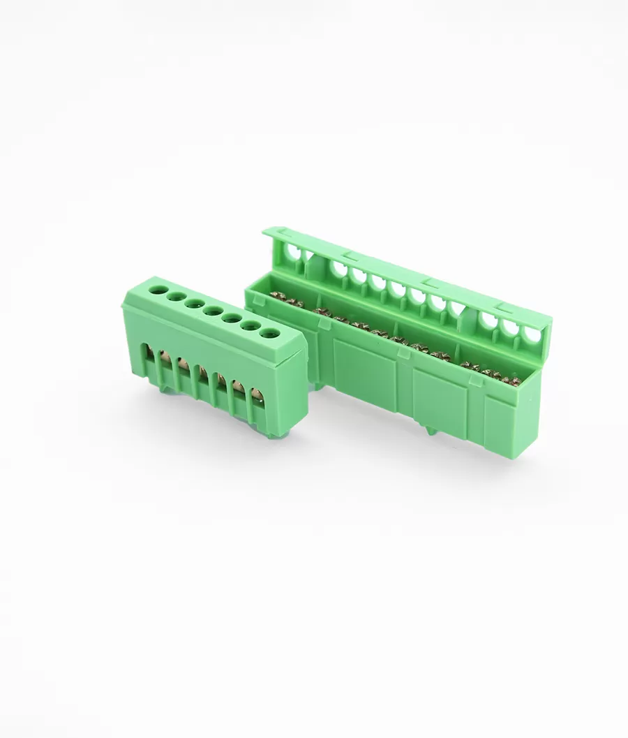
PCB Terminal Blocks: Footprints, Wire Entry and Soldering
Antong product selection reference · Updated 2 November 2026
A PCB terminal block connects field wiring to a printed circuit board. It has a wire-side connection and a board-side interface, both of which must fit the design. A pluggable PCB system adds a separate mating interface between a wired plug and a board header.
This guide explains board-level selection requirements. Antong’s SP010/SP011 catalogue entries describe pluggable screw terminal strips; they do not establish PCB pin dimensions, a recommended footprint or a soldering process for those products.
Start with the manufacturer footprint
- Confirm position count, row count and nominal pitch.
- Check pin cross-section, length, offsets and the specified hole or pad dimensions.
- Use the recommended tolerances and mounting features.
- Check the housing outline and installed height against nearby components and the enclosure.
- For a pluggable design, include both the fixed header and the matching wire-side plug.
A pitch value alone is insufficient. Two products can share a 5.08 mm pitch while using different pin layouts or mating geometries. Likewise, 5.00 mm and 5.08 mm are distinct dimensions; see the pitch guide for accumulated spacing error across a row.
Choose wire entry with the enclosure in view
Vertical, horizontal and angled entry options change where the conductor and tool need space. A compact board layout can become unserviceable if the final enclosure blocks the clamp or prevents a cable bend.
Model the actual conductor, any ferrule collar, screwdriver approach and plug-removal direction. The printed circuit board edge is not necessarily the final boundary: covers, ducts and neighboring modules can obstruct access after assembly.
Match the soldering process to the exact part
| Process | Selection question |
|---|---|
| Wave soldering | Is the specified part and pin arrangement approved for the intended wave process? |
| Through-hole reflow (THR) | Is this a reflow-qualified through-hole component with the required process limits? |
| Surface-mount reflow | Does the component have the documented pad design, packaging and reflow suitability? |
A through-hole pin does not automatically make a component suitable for reflow. Housing material, contact design and the stated thermal process limits must support the selected assembly method.
For an external example of the level of detail required, Phoenix Contact’s SPT-THR product page explicitly identifies pitch, pin information and THR/wave mounting. Those specifications belong to that Phoenix Contact product and must not be transferred to Antong strips.
Check the full current path
The terminal rating is only one part of a board assembly. The pins, solder joints, copper traces and any upstream protection must also suit the intended circuit. A high terminal current rating cannot compensate for an inadequate board connection.
Use the declared voltage conditions and the equipment’s insulation requirements when checking spacing. Neither a standard pitch nor the color of a connector proves adequate clearance or creepage in the finished device.
Test production and service conditions
Evaluate a representative assembly using the actual board thickness, solder process and wire. Inspect solder joints, tool access, cable loading and any plug retention. If operators will connect wires after the board is installed, test that exact sequence.
For a replacement, compare the complete mechanical drawing and approved mating pair. Matching a few visible dimensions is insufficient to approve a substitute.
Keep an Antong enquiry precise
If the requirement is a pluggable wire-to-wire strip, compare SP010 and SP011 using their own drawings. If it is a board-mounted product, state that explicitly and request the complete PCB specification before designing around a proposed part.
Provide the board drawing, required pitch and position count, conductor details, electrical conditions, entry direction, assembly process and quantity. A catalogue strip dimension should never be used as an improvised PCB footprint.
Product references
Model values above come from the linked Antong product pages. Confirm the ordered version and installation instructions before final selection.